Peking University, Mar. 16, 2015: Recently, Professor Wang Jian at Peking University and his collaborators discovered a new 2D superconductor with graphene or silicone-like structure formed by the substrate.
It is a two-atom layer crystalline Ga grown on GaN(0001) by molecular beam epitaxy (MBE). Both in situ scanning tunneling spectroscopy and ex situ electrical magnetotransport and magnetization measurements show the superconductivity in such two-atom layer crystalline Ga. The superconducting transition temperature TC is 5.4 K, which is 5 times higher than TC in stable bulk Ga phase. The graphene-like structure, which is totally different from Ga bulk structure, might also induce some interesting properties in this two dimensional material. Besides, GaN substrate is a wide used semiconductor in industry, our result demonstrates a pathway for exploring atomic-scale 2D superconductors by surface and interface engineering in a broad range of metal-semiconductor heterostructures, which benefit from present semiconductor technology and ultrathin film fabrication technique. The results were published in Physical Review Letters [PRL 114, 107003(2015) ] as an editors’ recommended paper.
Wang Jian and Ma Xu-Cun (Tsinghua University) are corresponding authors of this paper. Zhang Huimin (Physics Institute, CAS), Sun Yi (Peking University) and Li Wei (Tsinghua University) contributed equally to this work. The collaborators are professors Xue Qikun (Tsinghua University), Xie Xincheng (Peking University) etc.
The work was supported by National Basic Research Programs of China, National Natural Science Foundation of China, the Research Fund for the Doctoral Program of Higher Education (RFDP) of China, and Collaborative Innovation Center of Quantum Matter, China.
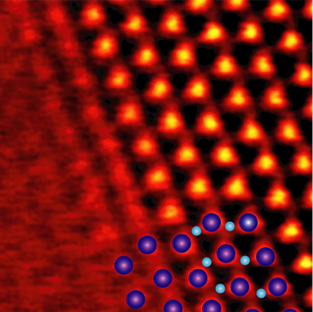
Figure 1. Transmission electron microscopy (TEM) image of the interface of two-atom layer Ga on GaN substrate.

Figure 2. Transport result showing an onset Tc of 5.4 K. The inset is a schematic measurement structure.
Edited by: Zhang Jiang
Source: International Center for Quantum Materials